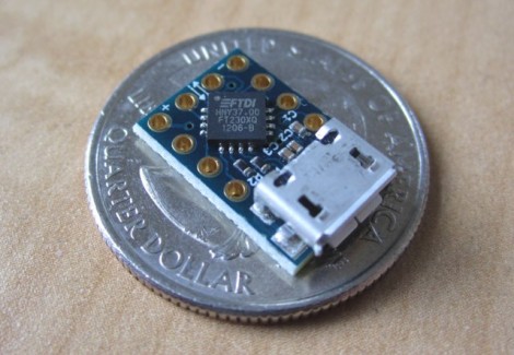
Using FTDI chips as a USB to Serial solution is nothing new, but this MicroFTX board takes the footprint to a new low. If you’re space limited this should have no problem fitting into your project. But if you plan to use it for prototyping we predict it’ll be lost in the parts bin forever as soon as you take your eyes off of it.
The USB Mini-B connector is becoming quite popular with hobby electronics these days. But here [Jim Paris] chose to use its little brother, the USB micro connector. Want to put this together by hand? How are you with 0402 footprints and QFN chips? In fact, there’s a ground pad on the bottom of that IC which means you really need to use a reflow oven to do the job right.
Aside from the diy-unfriendly fabrication size, we do like the design. There are four output pins (voltage, ground, TX, and RX) with a set of four solder jumpers to configure them. It can be powered from the USB port or an external connection, with the option for 5V or 3.3V output.
[Thanks John]


Could be even smaller is IC was on bottom 🙂
Or if the USB connector was on the bottom. 😀
You don’t have to use a reflow oven to get the QFN in place. All you need is a heat gun, a small vice for the PCB and a steady hand holding the components down with a pair of tweezers. I’ve replaced many components at work this way when the service department was backed up.
0402’s are easy… gets a bit more difficult with 0201’s.
In deed, 0402 is hard to hand-solder so that it looks perfect, but there are no problems getting it perfectly functional.
It’s this kind of articles that make people scared of SMD. Reflow ovens are only really necessary if you have a pick&place machine or for some speciality components.
A $50 chinese hot air solder station is nearly as good as a $1000 professional unit, the differences are mostly ergonomics and durability. The chinese one is not very comfortable to work all day with, and the heater can burn out in a few hundred hours.
You can get the 0402 to look almost perfect by using some flux on the work after you have done the initial soldering. Just add flux and touch the solder again with the iron — just make sure the tip is clean!
The word here is ‘almost’
I like the blue silk screen and diagonal layout. It adds some class to my projects.
To get an appreciation for how small this thing is, check out the layout (gerbers here). He’s managed to maintain 7mil trace and space which makes the board fairly easy to etch, but smaller than some fabricators will build at the lowest price tier. Nice work!
You can hand solder QFN’s with just flux and solder paste and an iron. I actually prefer the leadless chips, they’re a lot less likely to bridge and if they do you just push it away. just gently run the iron down the side.
don’t need ovens, plates or hot air.
they are even easier though with with paste and a hot plate, you can practically just drop them on and they’ll align themselves.
long pads help
http://farm6.static.flickr.com/5170/5327863563_4e345db3c8.jpg
How do you get the square GND pad on the bottom of the QFN to become soldered if you are not going to use a source of either a) hot air, or b) an oven?
The QFN’s that i work with (mainly power supply controllers) will burn up without a solid connection to a relatively large GND plane.
on these tiny chips the heat from the iron melts the paste (though i should have said leaded paste)
He was wise to chose the micro B connector. The USB Mini B is not recommended for future designs.
I missed that memo. I just designed a product with mini-B…argh. I’ll admit some resistance to the idea since I have so many mini-B devices around, and zero micro-B. But they claim it’s stronger, so I’ll swallow my pride.
I haven’t seen that either, I prefer the mini over the micro, the micro just breaks too much in my experience.
Are you sure its not Mini A and Mini A/B that has been deprecated (since 2007) and not Mini B.
Only in OTG has Mini B been deprecated for Micro, but anywhere else it seems like its still part of USB/IF
Unless it happened recently.
Yea, I’m sure. Most venders will warn you against it. It’s been this way for many years. There are a lot design advantages to micro B as well. For my DiY stuff it’s tough because it’s small, but it’s a better because it’s widely supported by the cell phone industry and over time I will have more micro B chargers, battery packs, and cables than mini stuff.
It’s not intuitive why micro is superior to mini B, but this is a good read.
http://electronics.stackexchange.com/questions/18552/why-was-mini-usb-deprecated-in-favor-of-micro-usb
Yeah all i see there is then talking about OTG and cellphones which Mini B is deprecated in.
2007 :
Mini B , Mini AB are deprecated
Mini B is deprecated in OTG, but not in USB/IF
http://www.usb.org/developers/Deprecation_Announcement_052507.pdf
darnit it, typo 🙂
Mini A , Mini AB are deprecated
not
Mini B , Mini AB are deprecated
It appears that you are correct. Document 4 of the 2.0 spec definitely agrees with you.
http://www.usb.org/developers/docs/
lol almost too small
When designing QFN boards(or anything with a ground pad) an easy way to solder them is run a via through the ground pad that you can touch from the bottom side. I just recently designed and built up a good 20 or so using that method.
Just make sure you can transfer enough heat if the pad is rather large.
the thing to watch for with that is that if you’re doing a hot plate/oven/factory run the solder can flow out of the vias
pretty much anything one-sided can be soldered with a clothing iron. or on the stove.
really, don’t discourage people like that. where’s the spirit?